 |
| February 13, 2018 | Volume 14 Issue 06 |
Electrical/Electronic News & Products
Designfax weekly eMagazine

Archives
Partners
Manufacturing Center
Product Spotlight
Modern Applications News
Metalworking Ideas For
Today's Job Shops
Tooling and Production
Strategies for large
metalworking plants
Board-level EMI shielding: DIY in minutes
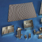 ProtoShield sheets from Tech-Etch are depth-etched with a checkerboard pattern for folding, so they can be easily formed into many diverse configurations. In the product-development stage, fully functional shields can be created in minutes with just a pair of scissors and a straight edge for folding. Offered in two sizes: standard (.25-in. squares) and metric (5-mm squares). Both versions are solderable and corrosion resistant due to nickel silver material. Shield prototypes can be directly soldered to the board, or shield clips can be used for easy mounting. Samples available.
Learn more.
Isolated probing tech for fast-switching power device testing
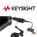 Keysight Technologies has developed an optically isolated differential probing family dedicated to enhancing efficiency and performance testing of fast-switching devices such as wide-bandgap GaN and SiC semiconductors. Validation of floating half-bridge and full-bridge architectures commonly used in power conversion, motor drives, and inverters requires measurement of small differential signals riding on high common-mode voltages. This measurement can be challenging due to voltage source fluctuations relative to ground, noise interference, and safety concerns.
Learn more.
Protect sensitive electronics in explosive environments with new aluminum ATEX Cabinet Cooler Systems
 EXAIR's ATEX Cabinet Cooler® Systems deliver a powerful and affordable solution for keeping electrical enclosures cool in hazardous ATEX classified areas -- and they're now available in durable aluminum construction. Engineered for use in Zones 2 and 22, these coolers are UL tested, CE compliant, and meet stringent ATEX standards for purged and pressurized enclosures. With cooling capacities up to 5,600 Btu/Hr., ATEX Cabinet Coolers are ideal for preventing overheating in electrical cabinets. EXAIR offers a comprehensive lineup of systems.
Learn more.
PLC handbook chock full of must-know information
 Automation-Direct's Practical Guide to Program-mable Logic Controllers Handbook has been improved with tons of new need-to-know info, making it a more comprehensive guide to the world of PLCs. Besides covering the basics of PLC history, PLC hardware, and PLC software, this guide takes you deeper into the ever-changing world of PLC communication, the importance of feedback loops, cyber security, and many other areas that are a must-know for any PLC novice or seasoned automation professional.
Get this great resource today.
Haptic feedback prototyping kit from TDK
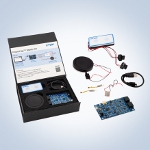 Get your customers to feel the difference your products make. TDK has released a development starter kit for fast haptics prototyping. It gives mechanical designers and engineers first impressions of the haptic feedback using PowerHap piezo actuators, shows how the mechanical integration works, and provides a reference design. Applications include automotive, displays and tablets, household appliances, vending machines, game controllers, industrial equipment, and medical devices.
Learn more.
Mini ESD preset torque screwdriver
 Need precision fastening with ESD protection at the smallest torque levels? Mountz has you covered. The new FG Mini ESD Preset Torque Screwdriver is built for low-torque, high-precision tasks. Its compact design makes it ideal for tight spaces and small fasteners, while delivering the same reliable control and ESD protection users have come to expect from Mountz. Two models available: FG25z (3 to 25 ozf.in, 2 to 17.7 cN-m) and FG50z (20 to 50 ozf.in, 14.1 to 35.3 cN-m).
Learn more.
Laumas load cells and electronics from AutomationDirect
 Automation-Direct has added Laumas precision-engineered load cells, transmitters, and accessories that deliver reliable performance in industrial weighing and force measurement applications. The FCAL series high-precision bending beam load cells are ideal for low- to mid-capacity systems. CTL series load cells are designed for both tension and compression, with excellent linearity. The CBL series low-profile compression load cells are perfect for space-limited applications. Laumas load cell transmitters are available too for precise monitoring and control. Very good pricing.
Learn more.
Engineer's Toolbox: What is ground loop feedback?
 Improper grounding can create problems in data logging, data acquisition, and measurement and control systems. One of the most common problems is known as ground loop feedback. Experts at CAS DataLoggers run through five ways to eliminate this problem.
Read the full article.
What is a braking resistor?
 According to Automation-Direct, "Braking resistors don't actually provide braking directly -- rather, they allow a drive to stop a loaded motor faster." Why is this important? Protect your AC or DC drive system from regenerative voltage that can create an over-voltage fault on the drive -- especially with high inertial loads or rapid deceleration.
View the video.
New Digital Static Meter: Precise measurement, easy use
 Static electricity isn't just a nuisance; it's a serious threat to manufacturing efficiency, product integrity, and workplace safety. Unchecked static can lead to costly downtime, product defects, material jams, and even hazardous shocks to employees. If static is interfering with your processes, EXAIR's upgraded Model 7905 Digital Static Meter offers an essential first step in identifying and eliminating the problem. With just the press of a button, this easy-to-use, handheld device pinpoints the highest voltage areas in your facility, helping you diagnose static issues before they become a problem.
Learn more.
New laser cutting modulating strategy tested with Mikrotron high-speed camera
 Modulating a laser beam's intensity distribution optimizes energy delivery to the process zone, resulting in better cutting speed, cut edge quality, and cut kerf geometry. Scientists in Belgium have come up with a new method that they say produces better cutting results.
Read the full article.
All-in-one embedded PLC based on Raspberry Pi 4 -- build control applications
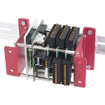 The new PLC CPI-PS10CM4 from Contec Co. is a compact embedded programmable logic controller (PLC) that is loaded with CODESYS, the world's most widely used software PLC. This product uses Contec's original single-board computer, which is based on Raspberry Pi's latest embedded module, the Compute Module 4 (CM4). By using the wide range of peripheral devices for Raspberry Pi, such as Contec's CPI Series, you can build various control applications in a PLC language that complies with the IEC 61131-3 international standard.
Learn more.
Torque sensors for fastening applications and more
 Saelig Company has introduced the Sensor Technology SGR525/526 Series Torque Sensors to provide precision torque monitoring that is critical for performance and safety. The square drive design (for applications with non-cylindrical shafts) allows for seamless integration into power tools, test rigs, industrial machinery, and precision fastening applications, ensuring superior torque measurement without the need for additional adapters or modifications. The SGR525 offers torque measurement only, while the SGR526 provides torque, speed, and power measurement using a 360-pulse-per-revolution encoder. Industries include automotive, aerospace, manufacturing, and research and development.
Learn more.
Wide-angle camera optimized for larger, faster conveyor belts
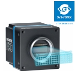 Wider conveyor belts operating at higher speeds are now commonplace in modern logistics. To keep up, SVS-Vistek is offering a cost-effective alternative to multi-camera systems with its fxo901CXGE 10-GigE color camera featuring the Sony IMX901-AQR wide-aspect global shutter 16.4-megapixel CMOS sensor. Unlike standard cameras, this unit captures targets in a wide field of view while maintaining high resolutions. The 4:1 horizontal aspect ratio allows one fxo901CXGE to replace an entire multi-camera system, removing the need for image synchronization.
Learn more.
Handheld thermal imager cuts diagnostic time
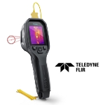 The FLIR TG268 is a next-generation thermal imager that provides professionals in the utility, manufacturing, electrical, automotive, and industrial sectors with a lightweight, handheld, affordable condition monitoring tool. Latest enhancements include higher temperature ranges, improved resolution, and larger data storage capacity. Go beyond the restrictions of single-spot IR thermometers to view and evaluate hot and cold spots that may signify potentially dangerous issues. Accurately measure temps from -25 to 400 C. Native thermal images improved with Super Resolution upscaling.
Learn more.
Researchers observe electrons zipping around in crystals
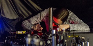
Calley Eads, a fifth-year doctoral student in the UA's Department of Chemistry and Biochemistry, aligns a laser system used to track electrons on time-scales at the limits of what can be measured. In her research, she investigates materials that could one day bring faster computing and more efficient solar cells. [Photo: Kyle Mittan/UANews]
By Daniel Stolte, University of Arizona
The end of the silicon age has begun. As computer chips approach the physical limits of miniaturization and power-hungry processors drive up energy costs, scientists are looking to a new crop of exotic materials that could foster a new generation of computing devices that promise to push performance to new heights while skimping on energy consumption.
Unlike current silicon-based electronics, which shed most of the energy they consume as waste heat, the future is all about low-power computing. Known as spintronics, this technology relies on a quantum physical property of electrons -- up or down spin -- to process and store information, rather than moving them around with electricity as conventional computing does.
On the quest to making spintronic devices a reality, scientists at the University of Arizona are studying an exotic crop of materials known as transition metal dichalcogenides, or TMDs. TMDs have exciting properties lending themselves to new ways of processing and storing information and could provide the basis of future transistors and photovoltaics -- and potentially even offer an avenue toward quantum computing.
For example, current silicon-based solar cells convert realistically only about 25 percent of sunlight into electricity, so efficiency is an issue, says Calley Eads, a fifth-year doctoral student in the UA's Department of Chemistry and Biochemistry who studies some of the properties of these new materials. "There could be a huge improvement there to harvest energy, and these materials could potentially do this," she says.
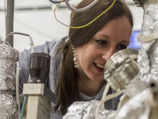
Calley Eads inspects a sample in the vacuum chamber to get it ready for measurement. [Photo: Kyle Mittan/UANews]
There is a catch, however: Most TMDs show their magic only in the form of sheets that are very large, but only one to three atoms thin. Such atomic layers are challenging enough to manufacture on a laboratory scale, let alone in industrial mass production.
Many efforts are underway to design atomically thin materials for quantum communication, low-power electronics, and solar cells, according to Oliver Monti, a professor in the department and Eads' adviser. Studying a TMD consisting of alternating layers of tin and sulfur, his research team recently discovered a possible shortcut, published in the journal Nature Communications.
"We show that for some of these properties, you don't need to go to the atomically thin sheets," he says. "You can go to the much more readily accessible crystalline form that's available off the shelf. Some of the properties are saved and survive."
Understanding electron movement
This, of course, could dramatically simplify device design.
"These materials are so unusual that we keep discovering more and more about them, and they are revealing some incredible features that we think we can use, but how do we know for sure?" Monti says. "One way to know is by understanding how electrons move around in these materials so we can develop new ways of manipulating them -- for example, with light instead of electrical current as conventional computers do."
To do this research, the team had to overcome a hurdle that never had been cleared before: figure out a way to "watch" individual electrons as they flow through the crystals.
"We built what is essentially a clock that can time moving electrons like a stopwatch," Monti says. "This allowed us to make the first direct observations of electrons move in crystals in real time. Until now, that had only been done indirectly, using theoretical models."
The work is an important step toward harnessing the unusual features that make TMDs intriguing candidates for future processing technology, because that requires a better understanding of how electrons behave and move around in them.
Monti's "stopwatch" makes it possible to track moving electrons at a resolution of a mere attosecond -- a billionth of a billionth of a second. Tracking electrons inside the crystals, the team made another discovery: The charge flow depends on direction, an observation that seems to fly in the face of physics.
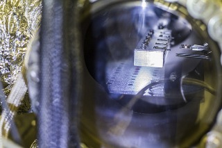
Extreme conditions are used to protect and preserve the TMDs during the experiments. As shown here, all samples are stored and manipulated in a vacuum that is close to the conditions in space. [Photo: Kyle Mittan/UANews]
Collaborating with Mahesh Neupane, a computational physicist at Army Research Laboratories, and Dennis Nordlund, an X-ray spectroscopy expert at Stanford University's SLAC National Accelerator Laboratory, Monti's team used a tunable, high-intensity X-ray source to excite individual electrons in their test samples and elevate them to very high energy levels.
"When an electron is excited in that way, it's the equivalent of a car that is being pushed from going 10 miles per hour to thousands of miles per hour," Monti explains. "It wants to get rid of that enormous energy and fall back down to its original energy level. That process is extremely short, and when that happens, it gives off a specific signature that we can pick up with our instruments."
The researchers were able to do this in a way that allowed them to distinguish whether the excited electrons stayed within the same layer of the material, or spread into adjacent layers across the crystal.
"We saw that electrons excited in this way scattered within the same layer and did so extremely fast, on the order of a few hundred attoseconds," Monti says.
In contrast, electrons that did cross into adjacent layers took more than 10 times longer to return to their ground energy state. The difference allowed the researchers to distinguish between the two populations.
"I was very excited to find that directional mechanism of charge distribution occurring within a layer, as opposed to across layers," says Eads, the paper's lead author. "That had never been observed before."
Closer to mass manufacturing
The X-ray "clock" used to track electrons is not part of the envisioned applications but a means to study the behavior of electrons inside them, Monti explains, a necessary first step in getting closer toward technology with the desired properties that could be mass-manufactured.
"One example of the unusual behavior we see in these materials is that an electron going to the right is not the same as an electron going to the left," he says. "That shouldn't happen -- according to physics of standard materials, going to the left or the right is the exact same thing. However, for these materials that is not true."
This directionality is an example of what makes TMDs intriguing to scientists, because it could be used to encode information.
"Moving to the right could be encoded as 'one' and going to the left as 'zero,'" Monti says. "So if I can generate electrons that neatly go to the right, I've written a bunch of ones, and if I can generate electrons that neatly go to the left, I have generated a bunch of zeroes."
Instead of applying electrical current, engineers could manipulate electrons in this way using light such as a laser, to optically write, read, and process information. And perhaps someday it may even become possible to optically entangle information, clearing the way to quantum computing.
"Every year, more and more discoveries are occurring in these materials," Eads says. "They are exploding in terms of what kinds of electronic properties you can observe in them. There is a whole spectrum of ways in which they can function, from superconducting, semiconducting, to insulating, and possibly more."
The research described here is just one way of probing the unexpected, exciting properties of layered TMD crystals, according to Monti.
"If you did this experiment in silicon, you wouldn't see any of this," he says. "Silicon will always behave like a three-dimensional crystal, no matter what you do. It's all about the layering."
Published February 2018
Rate this article
View our terms of use and privacy policy